
Backside grinding and ultra-thinning down to low profiles for full/partial wafers, bumped substrates, reticles, and single die — held to ±10 µm thickness accuracy and surfaces down to Ra 0.009 µm. Stocking seven wheel varieties and protective tapes, we match processes to your exact substrate and device topology, including thinning of bumped wafers.
On bumped wafers we thin over bumps and pillars as small as 250 µm, matching the wheel and mount to each device topology.
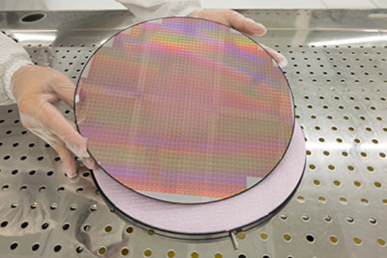
Every job is characterized to the customer's substrate and target thickness. Representative limits:
| Parameter | Capability |
|---|---|
| Substrates | Si · SiGe · SOI · SiC · Garnet |
| Wafer diameter | Up to 300 mm |
| Wafer thickness | 5 mm down to 25 µm |
| Minimum thickness | 25 µm |
| Accuracy | ± 10 µm |
| Surface roughness | Ra 0.009 µm |
| Grinding wheels | 7 varieties |
| Ball-bump thinning | over ≤ 250 µm bumps / pillars |
| Die & reticle thinning | Yes |
Our DAG810 grinder handles 300 mm wafer thinning on a single, high-flexibility spindle with an in-process height gauge for live thickness monitoring. It also supports frame grinding and individual die thinning, holding accuracy within 10 µm.
For wafers prone to backside chipping or cracking, DBG pairs grinding with dicing: the wafer is trenched (diced deeper than the final thickness) and then ground down until the die singulate. The result is cleaner die edges on fragile substrates.